Sapphire, due to its unique physical properties, can be used for the manufacture of optical products operating under extreme conditions, i.e. when exposed to high temperatures, pressures, mechanical loads, corrosive environments and radiation.
For the successful application of optical products, the quality of the polished surface is critical. The previously existing sapphire polishing technology, which was characterized by the use of heavy chemical effect, led to a sufficiently high class of surface roughness (Ra about 10A), but did not provide any optically sufficient irregularity, even for flat windows. Products made using this technology are widely used in the clockwork industry, electronics, etc., but are rarely suitable for precision optical instruments.
Components for devices have traditionally been manufactured by mechanical processing, which led to a higher accuracy of the surface shape, but did not provide high parameters of optical purity and roughness.
The main difficulty in combining mechanical and chemical processing was that the applied suspensions - sapphire etchants - destroyed the materials of the polishing tool.
As a result of research carried out in our company, a new technology of chemical-mechanical polishing of sapphire has been developed, which provides a minimum roughness and, at the same time, high requirements for the purity and surface irregularity.
Surface roughness
The surface roughness during the polishing process was monitored using a Solver Pro atomic force microscope (AFM).
The figures show the profilograms of the roughness of the polished surfaces of the samples for different stages of their processing according to our technology.
As can be seen from the figures, with the course of processing time, both the roughness and the surface structure change - the roughness decreases, and the structure becomes more uniform.
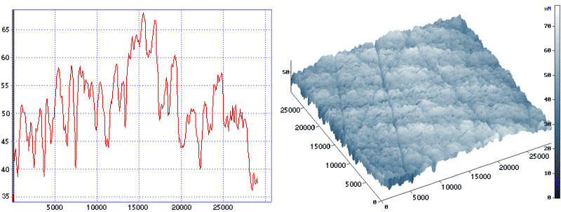 2D and 3D profiles for 15 minutes of processing time (Ra = 6.046 nm)
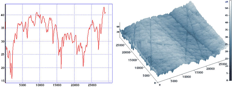 2D and 3D profiles for 30 minutes of processing time (Ra = 4.218 nm)
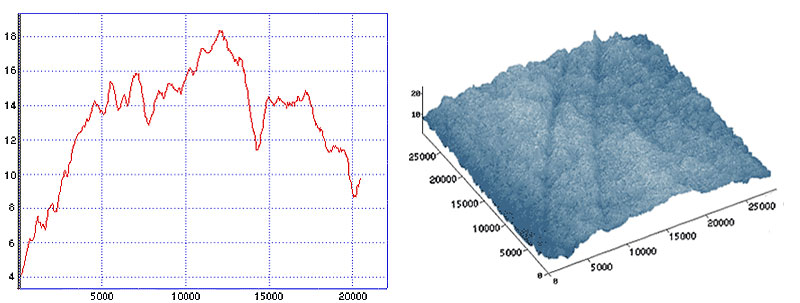 2D and 3D profiles for 60 minutes of processing time (Ra = 2.001 nm)
") 2D and 3D profiles for 90 minutes of processing time (Ra = 1.31 nm)
2D and 3D profiles for 90 minutes of processing time (Ra = 1.31 nm) 2D and 3D profiles for 240 minutes of processing time (Ra = 0.969 nm)
The resulting roughness Ra is 9 A, which corresponds to the best samples of products, to which other manufacturers do not impose requirements for the accuracy of the surface shape. Such a low roughness value with the simultaneous absence of "hair" scratches virtually eliminates light scattering, which is especially important for laser applications. Our technology manages to simultaneously obtain high values of surface accuracy - see below.
A complicating factor in the precise processing of sapphire is the anisotropy of its mechanical and other physical properties. It has the least effect on plane surfaces, thus for the planes the best results are achieved. Hemispherical domes and microlenses are the most complex of all spherical surfaces. The technology has been developed for hemispherical domes and microlenses ranging in size from 3 mm to 180 mm and wall thickness, respectively, from 0.25 mm to 6 mm.
Plane windows
The developed technology is used to produce windows with a diameter of up to 250 mm, the surface shape accuracy of which (propagating TWD wavefront or flatness) is up to 0.1 lambda (lambda 633 nm), and the surface purity is 20/10 MIL.
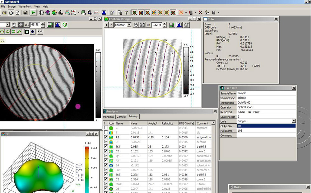
Interferogram of the transmitted wavefront for a sapphire window with the following parameters:
- Diameter: 120mm;
- Thickness: 15mm;
- Purity class: 20/10 MIL.

Hemispherical domes
The technology was developed and batches of domes with a diameter of 10 to 200 mm, with a wall thickness of 2 mm and with the following average parameters were manufactured:
- Thickness variation throughout the product - 0.02 mm;
- Surface irregularity: in the central zone - 0.5 lambda, in the edge zones - 1-1.5 lambda;
- Purity class - 60/40 MIL;
 Interferogram of the inner surface of a dome (cowl) made of optical sapphire. R = 79.995 (Center zone Ø50 mm)
 Interferogram of the inner surface of a dome (cowl) made of optical sapphire. R = 79.995 (Edge area Ø50 mm)
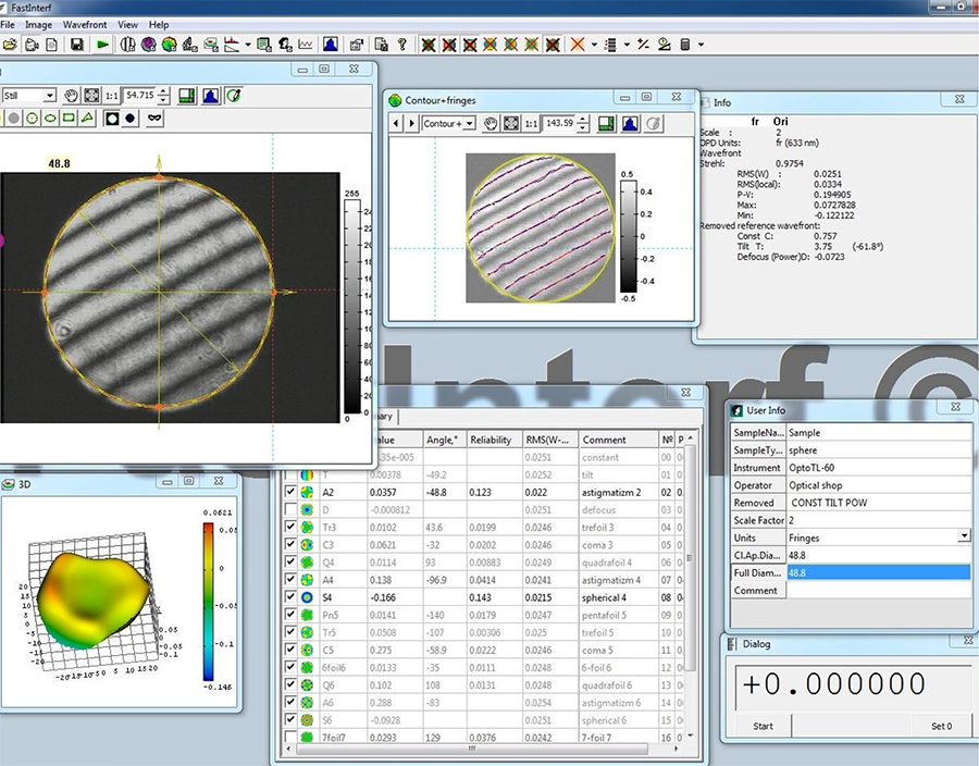
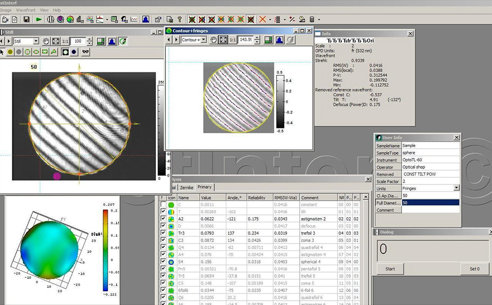 Interferogram of the outer surface of a dome (cowl) made of optical sapphire. R = 85.015 (Center zone Ø50 mm)
 из оптического сапфира. R=85.015 (Краевая зона Ø50 мм)") Interferogram of the outer surface of a dome (cowl) made of optical sapphire. R = 85.015 (Edge area Ø50 mm)
Interferogram of the outer surface of a dome (cowl) made of optical sapphire. R = 85.015 (Edge area Ø50 mm) Photo of a dome (cowl) made of optical sapphire, diameter 170 mm, as well as domes with a diameter of 48 mm and 20 mm
Lenses
- Diameter - 5-250 mm
- Surface irregularity - up to 0.1 lambda
- Purity class 20/10 MIL
 Sapphire lens surface interferogram
Opto-Technological Laboratory Ltd (Opto-TL) is innovative production enterprise founded in 2002. Main activity – design and manufacturing of optical products.
Quality Management System applied to development, manufacturing and service of optical components out of crystals and glasses, optical systems (including objectives), optical testing and measuring devices corresponds to GOST R ISO 9001-2015.
Contact information
Phone: +7 (812) 347-76-90
E-mail: sales@optotl.ru
For technical questions: technical_service@optotl.ru
2026 © Opto-Technological Laboratory» Ltd
Made by SOTBI